


 Functional Diagram
Features
- 700 MP/s ISP Processing throughput
- Supports multi-camera input
- Low latency ISP processing
- eWarp® geometric processor
- 8MP60 (480 MP/s) H.264 encoder
- Quad core ARM® Cortex A53 applications processor
- 2.5 TOPS (NPU + DSP)
- Software Development Kit
- 32-bit LPDDR4(x) DRAM interface
- ASIL-B compliant
- Supports HSM for cybersecurity needs
- Automotive qualified (AECQ-100 Grade-2)
Applications
Automotive
- Advanced Driver Assistance Systems (ADAS)
- Single/Multi-camera eMirror Systems
- Driver & Occupant Monitoring systems (DMS/ OMS)
- Parking assistance camera systems
- Smart Back-up Camera
- Ethernet encoding cameras
Industrial and Consumer
- Smart cameras for AMRs and Humanoids
- High-speed smart industrial cameras
- Barcode and QR readers
- Biometric cameras
- 3D and 360-deg vision systems
- Dash cameras
Functional Diagram

The iND881xx smart camera video processor (CVP) SoC builds on the world-class image processing (ISP) capabilities of the iND880xx by incorporating a low-power, heterogeneous AI compute engine to enable smart cameras for automotive and non-automotive applications. The multi-sensor high dynamic range ISP can simultaneously process multi-camera input streams with low-latency (sub-1ms).
The ISP feeds a 2.5 TOPS neural processing unit (NPU) and DSP optimized for real-time vision processing tasks. This enables rapid and precise video analysis, object detection, and scene understanding for driver and occupant monitoring, pedestrian detection and more. Designed to operate on the edge, the iND881xx offloads the central compute device, freeing resources for critical system tasks.
The iND881xx also integrates an H.264 encoder, application processor, and hardware security engine, with the flexibility to handle a wide range of sensor inputs—including thermal, depth, IR, and radar. An accompanying SDK streamlines development, enabling designers to bring products to market more quickly.
iND881xx enables a wide range of use cases—from in-cabin monitoring (DMS/OMS/DOMS) and advanced driver assistance systems (ADAS)to smart industrial and retail cameras, 3D sensing, and multimodal sensor fusion—making it a versatile platform for next-generation smart sensing applications.
| Device Name | Pixel Rate (Max.) | NPU | DSP | Application Processor | DRAM Interface |
|---|---|---|---|---|---|
| iND88140 | 700MP/s | 2 TOPS | 500 GOPS | Quad A53 | LPDDR4(x) 32-bit @ 2.1 GHz |
| iND88120 | 350MP/s | 1 TOPS | 300 GOPS | Dual A53 | LPDDR4(x) 32-bit @ 1.4 GHz |
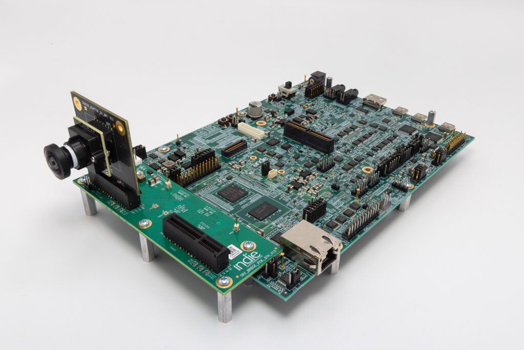
Evaluation Kit
indie offers Evaluation Kits (EVKs) for our Camera Video Processors (CVPs), to accelerate development through rapid prototyping and performance evaluation. For more information, please contact our sales department [email protected].
Multi-stream Fully Independent and Configurable High Dynamic Range Image Signal Processor (ISP)
- High speed multi-channel 24-bit ISP
- Less than 1ms ISP processing latency
- Up to 700 MPixels/ second processing
- Multi-camera support
- Advanced color filter array processing
- RGB-IR, RGGB, RCCB, RCCG, RYYCy, RCCC, Thermal, Monochrome
- Optimized RGB-IR (4×4 only)
- High Dynamic Range (HDR) support
- 144 dB HDR 24-bit pipeline
- 2 and 3 exposure on-chip combiner
- Advanced Local Tone Mapping
- Simultaneous support for different frame rates, resolutions, and CFAs
- Advanced spatial (2D) noise reduction
- Zone-based statistics for AE and AWB
- Color noise reduction
eWARP Geometric Processor
- Proprietary 6th-gen eWARP® geometric processor
- Independently dewarps up to two 200+ degree videos
- Ultra-wide field of view (FOV) lens distortion correction
- Ultra-low latency (typically 1/6th of a frame)
- Dynamic Electronic Pan/Tilt/Zoom (ePTZ)
- Lens distortion, perspective, and alignment correction
Neural Processing Unit
- 2 TOPS at 1 GHz / 1024 GMAC [8×8]
- 768 KiB Tightly coupled memory
- Supports unstructured sparsity to reduce memory bandwidth and power while increasing performance
Floating-point VLIW SIMD DSP
- 500 GOPS / 70 GFLOPS / 205 GMAC [8×8]
- 16-way 32b single precision float data
- 512b-wide SIMD instruction capability
- 64 KiB instruction cache, 64 KiB data cache
- 256 KiB tightly coupled memory
- Native instruction set for non-linear math operations
- 0.5 TOPS AI engine
QuadCore ARM® A53 Neon™ Application Processors
- Ability to run up to 1GHz (10k DMIPS)
- 32 KiB Data / 32 KiB Instruction cache per core
- Unified 512 KiB L2 cache
- FPU & NEON extensions
Software
- Software Development Kit (SDK)
- SDK included code libraries, APIs, compiler, interpreter, debugger, testing tools, sample code, build tools, IDE, drivers, reference camera tuning
- Easy-to-use Linux-based SDK for flexible application development on ARM cores
- RTOS support on LX7 cores for safety-critical software
- Computer Vision library to accelerate classical vision algorithms
H.264 HW Encoder
- I- and I/P-frame support
- Up to 8MP at 60fps support (480MP/s)
- Slice based encoding for low latency
- Hierarchical motion vector search for better image quality
Graphics Display Processor
- Scaling, compositing, and blending
- 2D graphics engine supports 2x 1920×1080 at 60fps
- Tessellation engine for lines, quadratic and cubic Bezier curves
- Imaging and pixel engines for rendering and compositing
- Animated bitmap and scalable vector graphics support
Dedicated Hardware Security Module and Safety Island
- Dual core lock step RISC processor for
- security and safety
- Secure processing and memory environment
- Cryptographic functions: asymmetric/symmetric
- key encryption and hashing
- Secure boot
- Key provisioning mechanisms
- True Random Number Generator (TRNG)
- Secure debug
- Signature verification on video input
- Signature addition on output streams
- One Time Programming (OTP) memory
Dual 32-bit RISC Tensilica™ LX7 Microprocessor
- Operation up to 714 MHz
- Floating point and multiply/divide accelerators
- 32 KB Instruction cache/32 KB data cache per core
Video Inputs
- Dual 10 Gbps (4-lane @2.5Gbps/ lane) (MIPI D-PHY)
- Supports up to RAW24 and YUV 4:2:2-12
- 16 virtual channels per port
- 16-bit parallel interface
Video Outputs
- Single 10 Gbps (4-lane @ 2.5 Gbps/ lane) MIPI D-PHY or 17.1 Gbps (3x trios @ 2.5 Gsps/ lane) MIPI C-PHY
- 8 Virtual channels on MIPI output
- Additional OpenLDI output interface
- Customizable embedded data in video stream
- Supports various RGB and YUV formats
- 16-bit parallel interface
System Interfaces
- Four SPI controllers
- Two independent SPI controllers to connect to QSPI- NOR and OSPI-NAND boot flash
- One additional QSPI master controller
- One SPI Slave controller
- One SD/ SDIO/ eMMC interface
- One 100/1000 Ethernet with RGMII
- Four Inter-Integrated Circuit (I2C™) ports
- (2x master and 2x slave)
- Dual CAN 2.0/CAN-FD ports
- Four UARTs
- Three pulse width modulators (PWM)
- Seventeen dedicated GPIO/GPO
- JTAG port (IEEE Standard 1149.1-1990)
- 32-bit LPDDR4(x) interface with inline ECC
- I2S input and output interface
Safety Features
- Support for hostless safety designs with customizable failure recovery management
- Customizable safety pin for host assisted safety design
- ECC support for all processor code spaces
- Interface support for error detection & correction modes
- Windowed Watch Dog Timer
- Power, reset, and clock management
- Process, voltage, and temperature sensors
- ISO 26262 ASIL-B (for automotive)
- 2-channel ADC for external voltage measurement
Electrical Specifications
- Core supply voltage: 0.8V ±5%
- I/O supply voltages: 1.8V and optional 3.3V ±5%
- PLL supply voltage: 1.8V ±5%
- MIPI supply voltage: 0.8V and 1.8V ±5%
- LPDDR4 voltage: 1.1V and optional 0.6V for LPDDR4X
Package
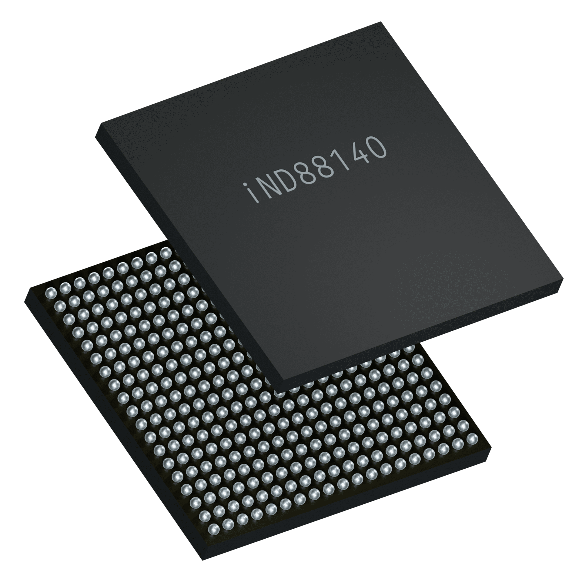
- 361-ball FC-CSP, 13mm x 13mm, 0.65mm pitch